
(Disclaimer: This article has not been simplified for a general audience and thus employs a large amount of technobabble and takes knowledge of low level computer logic for granted, beware)
For a number of years now, the idea of making my own computer at a hardware level fascinated me.
The idea of using discrete logic gates, which is only one level ‘above’ transistors, to do computation (something that modern computers still do to this day at a fundamental level), I find amazing.
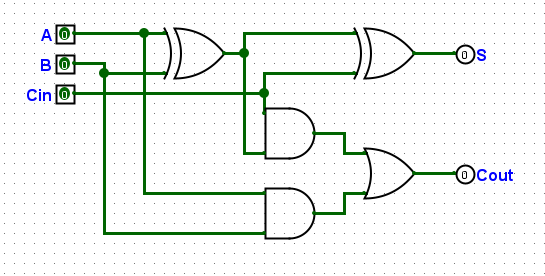
So, one very boring Thursday evening, after being inspired and building a 4 bit adder, I thought “Why not take it a step further” and began attempting to turn it into what I think a computer is.
3 Hours of faffing about later and I had QND V1 complete:
It’s very primitive, but it does work.
And since it was made over the course of a few hours using a very rudimentary understanding of how computers are supposed to do, I have named it QND.
QND standing, of course, for Quick N’ Dirty.
It features:
- Random, Made on the fly assembly
- Multiplexer Hell
- 16 * 12 bits of programming memory
- 16 * 4 bits of random access memory
- 60% functional ALU steering
- Calculations!
I programmed it with a single program, which was written at the same time as the control unit to make it work was being wired, which is why the first 4 bits mainly iterate upwards.
Also note that V1 only used a 3 bit instruction set, the first bit is ignored.
You may notice that I use prebuilt RAM and ROM modules.
This is because I did this for entertainment and learning, not tedium.
Understanding how memory works is one thing, wiring up 4,096 of the buggers is a whole different chestnut.
This program calculates then returns 2 + 3 – 1, then halts.
1001 0001 0010 // write 0010 to adr 0001
1001 0010 0011 //write 0011 to adr 0010
1010 0001 0000 //read adr 0001
1011 0001 0000 //write adr 0001 to a
1010 0010 0000 //read adr 0010
1100 0010 0000 //write adr 0010 to b
1101 0011 0000 //write a + b to 0011
1001 0101 0001 //write 0001 to 0101
1010 0101 0000 //read adr 0101
1100 0101 0000 //write 0101 to b
1010 0011 0000 //read 0011
1011 0011 0000 // write 0011 to a
0110 0100 0000 //write a - b to 0100
1010 0100 0000 //read 0111
1111 0000 0000 //halt
(Note: Might not actually be the original program)
Here is a video of it running at 0.5hz:
After that exhilarating and high octane demonstration, we once again return to the boring explanations.
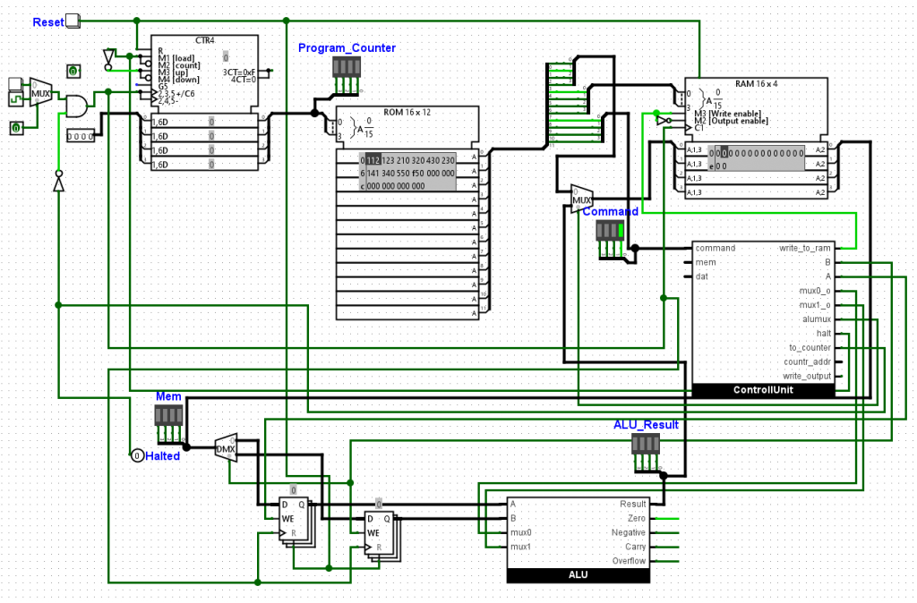
Here are some diagrams of the various components:
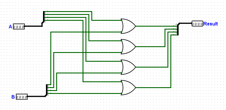
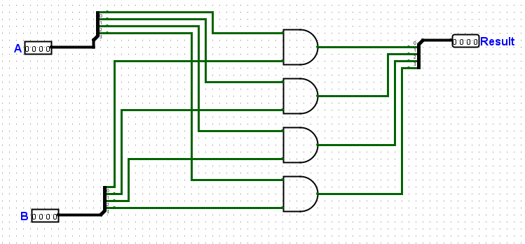
What it basically does is:
The program counter just ticks up and up and up, this cycles trough all 16 ROM locations, which can load a value into memory, load a value from memory into the ALU, and load a value from the ALU into memory.
That’s about it really.
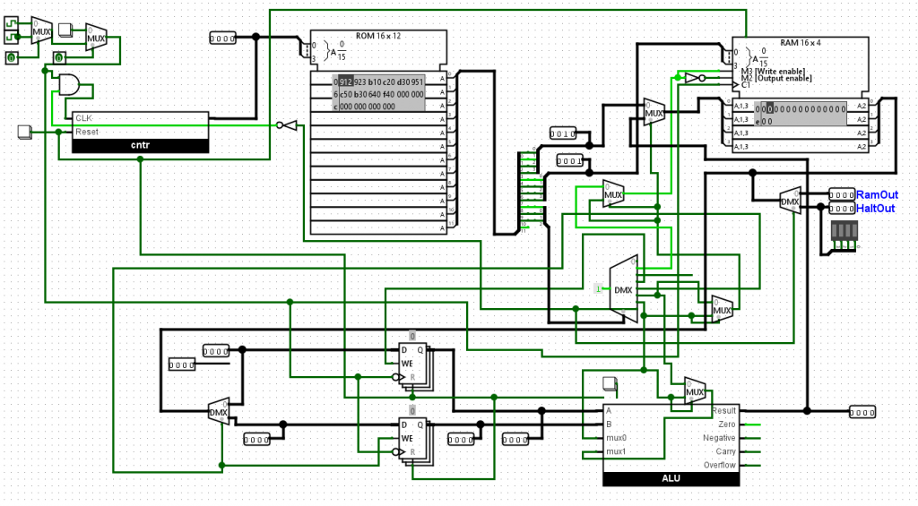
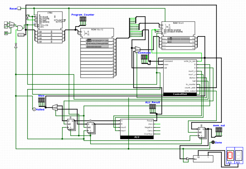
But I was not yet satiated, and really didn’t like the MUX spaghetti I had created, so the next day I created V2.
This included the CU (Control Unit) Integrated into a neat package like the rest, making it all look quite neat.
Later sub-version V2.5 also incorporate a 2 digit 7 seg display for those who can 0 read binary.
And a connection from the CU to the updated programming counter, meaning it can conditionally loop which in turn allows it to do fun stuff such as multiplication!
Speaking of the CU, here it is:
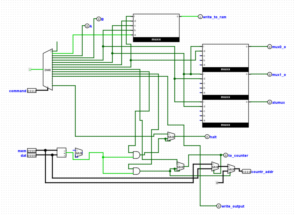
Wonder whats inside those muxx blocks?
Well…
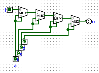
Yeah.
For V3 those were replaces by the OR gates they should have been to begin with.
Now the CU basically turns the (now) 4 instruction bits into the appropriate pins, so the ram chip can be set to read from memory for example.
Here is a basic flow diagram of V2 onward:
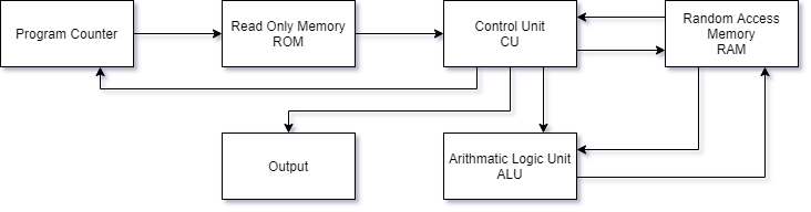
So: The program counter goes trough the ROM, which gives instructions and data to the CU, which in turns communicates those instructions to the RAM and ALU to move and calculate what is instructed and to where.
Simple right.
Here is a simple program that calculates 4 * 3:
0001 0001 0011 //move 3 to m1
0010 0001 0000 //move m1 to a
0011 0010 0000 //move m2 to b
0100 0010 0000 //move a + b to m2
0001 0011 0001 //move 1 to m3
0010 0011 0000 //move m3 to a
0011 0100 0000 //move m4 to b
0100 0100 0000 //move a + b to m4
1011 0010 0000 //move m2 to out
1001 0100 0100 //halt if m4 = 4
1010 0000 0000 //repeat if m0 = 0
I want to take some more of your time away to attempt to explain the fancy numbers I just spit onto your retinas.
It goes as follows:
4 bit instruction, 4 bit address, 4 bit data
So, for line 1 up there
0001 (instruction 1) 0001 (memory address 1) 0011 (data 3)
Which results in moving ‘3’ to memory address 1
The program itself uses some of this fancy new 4 bit instruction set to do multiplication, which is implemented as follows:
Do total + 3
Do counter + 1
Repeat Until counter is 4
Then print total
This is simplified of course, but if you want it un-simplified simply decipher the program itself.
Complaints can be sent here, by the way.
Here is said program in action:
Anyhow, this is all well and good, but I can still only work with 4 bit numbers, and my favorite number is above 15.
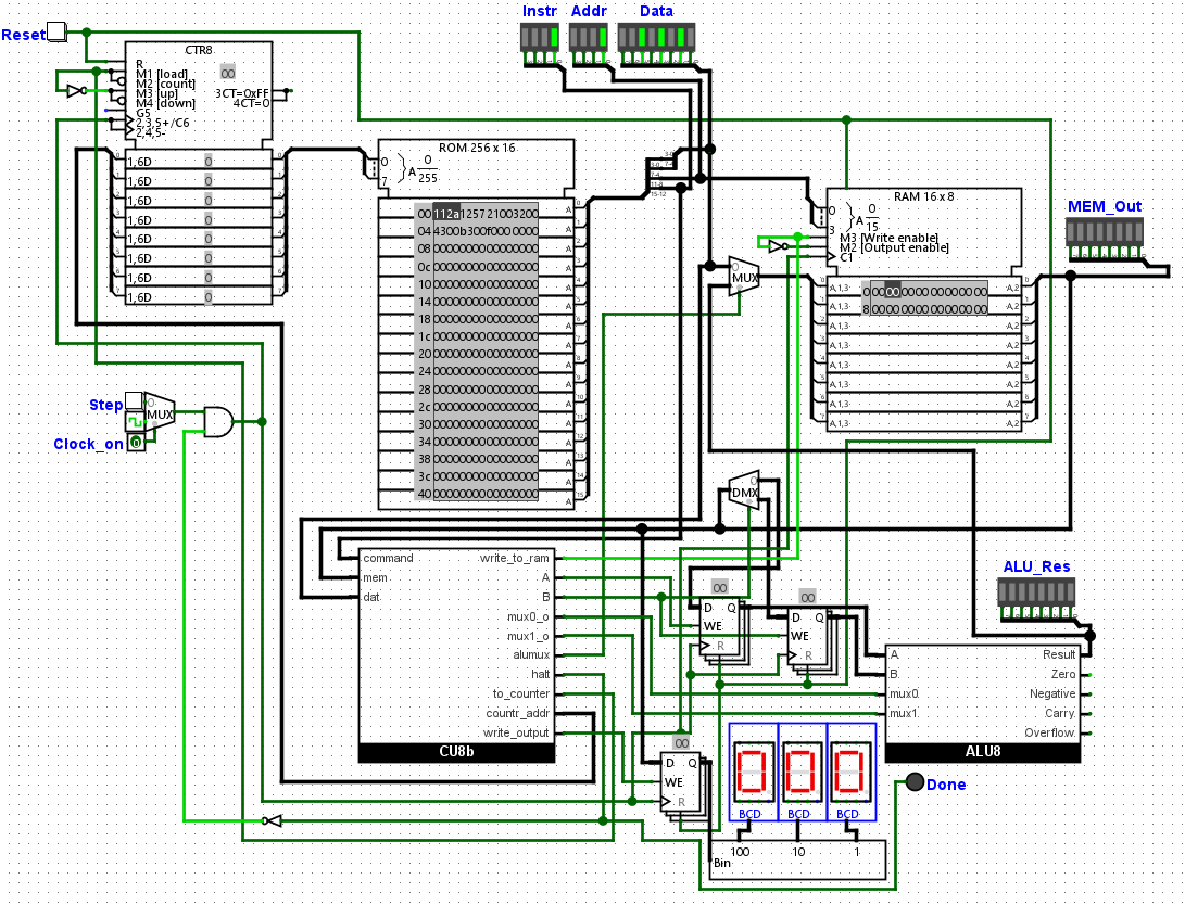
Now, worry no more! for version 3 is now available!

Now, this uses the same instruction set (Albeit a further iterated on version), and still has a 4 bit address system for the ram.
This is out of laziness.
It also has a 8 Bit program counter and memory size, allowing for far longer programs and working with numbers up to 255!
This, too, is out of laziness.
Because by having a mere 4 bits of memory I can keep the program strings 16 bits long (4 instruction, 4 address, 8 data) which is shorter and thus easier to work with.
And because by having the data and program counter at the same length, I can not only have longer programs, but can also directly pump the data to the program counter without having to do any conversion (or thinking)
Speaking of laziness, programming the damn thing!
Cause so far, I have written out the programs in binary, which I then converted per line to hexadecimal, which I then entered 1 by 1 into the ROM.
That simply would not do.
So, I hereby present: Dennesembly (Patent Pending)
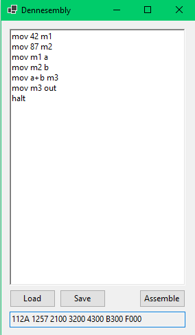
Cause, I noticed that while writing the comments for my code, I went from “Write to memory adress 1” to “move to memory 1”, to just “mov mem 1”.
And I thought: This looks like assembly!*
*May not actually look like assembly, I don’t know assembly
So I went at it, and a hour or so later I had bashed together some C# to convert a simple and limited assembly language of my own design to binary, and subsequently to a string of hexadecimal compatible with Logisim’s ROM module.
It’s very crude, but I can justify that because I am the only user.
If I were to ever release it I would of course clean it up and document it, but until then its a tool for a job and it works well enough for that.
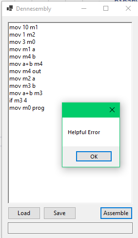
Here is 4 * 10 in Dennesembly™
mov 10 m1
mov 1 m2
mov 3 m0
mov m1 a
mov m4 b
mov a+b m4
mov m4 out
mov m2 a
mov m3 b
mov a+b m3
if m3 4
mov m0 prog
Speaks for itself really.
(prog in this case is the program address, making it what amounts to a jump statement)
This spits out 110A 1201 1003 2100 3400 4400 B400 2200 3300 4300 9304 8000, which is the hexadecimal representation of the instructions.
Basically, it works.
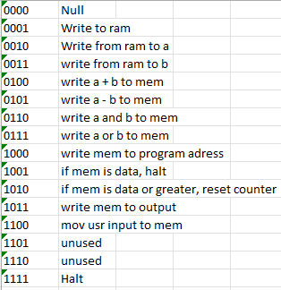
Speaking of the instructions, for the V2 upgrade I actually planned them out, and by V3 they looked like this:
And here is an early program written in binary, with the comments that inspired Dennesembly™
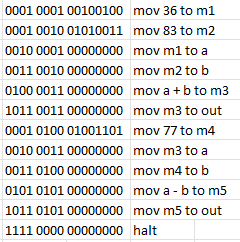
And here is that program in action:
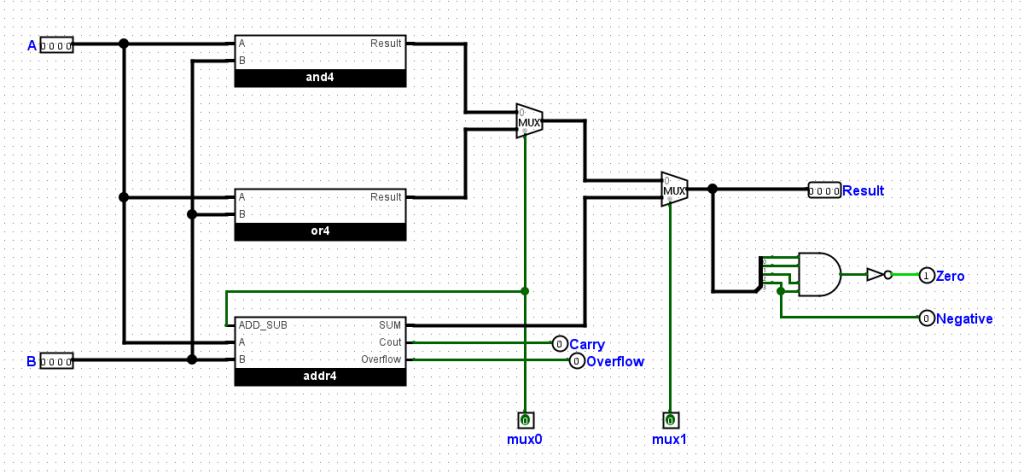
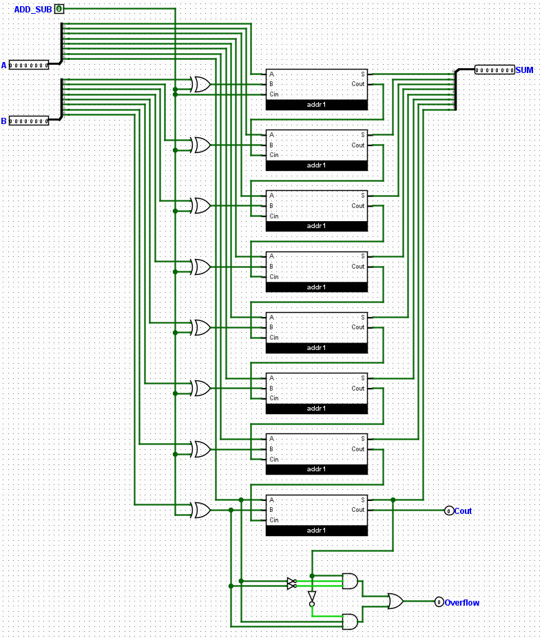
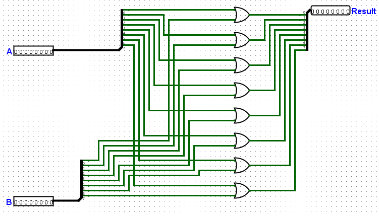
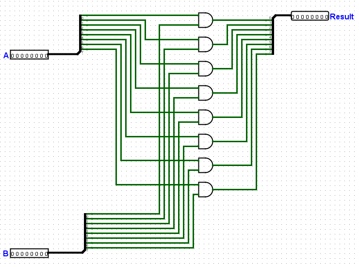
Here is the new 8 bit ALU, mainly cause I like the wiring

Oh, and not to forget, the computer itself is made in Logisim.
Specifically the open source continuation Logisim-Evolution.
If you want to faff about with digital logic, and redstone ain’t cutting it, I can highly recommend it!
And if you are a scientist who could use it for its intended purpose, you already have it.
That’s about it really.
I might publish the computer and Dennesembler™ later, after extensive cleanup.
I might also not, I do forget.
And since I stole referenced so much (read: most) of the ALU design from the internet I thought it would be best to make a sources section:
| How to make a adder / subtractor (Only the images) |
| The entire ALU Design (Again, by sight) |
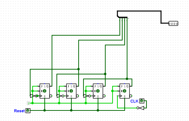
| Program counter (Only the schematics, notice a theme?) |
That will be all.